Recently, thermal assessment has become a popular topic in power management system. With the increasing power requirements for many applications, thermal management should be considered to avoid overheating. Especially for dc-dc converter products which combine power MOSFETs in the chip, the power dissipation is facing challenges of limited size of package and PCB layout area. Therefore, the thermal assessment should be included in the project preview. The Flotherm is a professional thermal simulation tool to simulate the real condition of a thermal system, and it can help to reduce the unnecessary cost of trial and error process. In this application note, the modeling and verification of thermal model for power management system will be discussed.
1.
Modeling of
Thermal Model for IC
There are many kinds of IC packages based on different applications and requirements. Several parameters such as package size, construction, materials, die size, and power dissipation profile will affect the thermal resistance of IC. Generally, these parameters can be provided by IC Product Engineer (PE), and the thermal model can be developed based on the parameters mentioned above. Following are some common IC packages applied for DC-DC Buck Converters and PMICs.
Figure 1. Different Types of IC Package
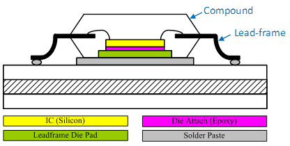
Figure 2. An Example of Thermal Model Construction
Figure 2 is an example of thermal model construction for a chip mounted on the PCB. The thermal model of IC consists of die, die attach, lead-frame die pad and solder paste, and each of them has different thermal conductivity based on their materials. Generally, the material of die is silicon, and its conductivity is 117.5 W/(K·m). Other materials properties can be referred to the Table 1 as below for example. Thermal conductivity may change with different materials. Note that the (absolute) thermal resistance in K/W of an object depends on the thermal conductivity, the length and the cross-section of the thermal path:  where θ is the absolute thermal resistance, ∆l is the length of the thermal path, A is the cross-section area of the thermal path and k is the thermal conductivity of the material.
Table 1. Thermal Conductivity of IC Thermal Model
|
Items
|
Materials
|
Thermal Conductivity
|
|
Die
|
Silicon
|
117.5W/(K·m)
|
|
Die attach
|
Epoxy
|
2.5 W/(K·m)
|
|
Lead-frame die pad
|
Copper
|
385 W/(K·m)
|
|
Lead-frame
|
Copper
|
385 W/(K·m)
|
|
Solder Paste
|
Sn63/Pb37
|
50.9 W/(K·m)
|
|
Compound
|
G700
|
0.9 W/(K·m)
|
2.
Modeling of
Thermal Model for Inductor
Except for the IC, the inductor can be seen as the second large heat source in a switch-mode power converter system. Therefore, the development of inductor thermal model is essential. Similar to the model of the IC, there is some information required to establish an accurate inductor thermal model. First, we can find the outline dimension of inductor in datasheet, including the length, width and height (See Figure 3.). Second, the internal structure is invisible due to outer obstruction. There are two methods to get the required parameters. One is to demolish the inductor to measure the internal wiring configuration such as wire thickness and the number of turns. Another more gentle method is asking the inductor manufacture for the information. Then you can follow the information to establish the thermal model of inductor as Figure 4 and Figure 5.
Figure 3. Outline Dimension of Inductor
Figure 4. Inductor Internal Construction Provided by Manufacture
Figure 5. Inductor Thermal Model Developed by Flotherm
The thermal conductivity of inductor materials are listed in Table 2. It should be noticed that most of heat will transfer through copper wire to external power trace. This is because the thermal conductivity of copper is higher than the ferrite, so the majority of heat will flow via the route with highest thermal conductivity.
Table 2. Thermal Conductivity of Inductor Thermal Model
|
Material
|
Thermal Conductivity
|
|
Ferrite
|
4.353 W/(K·m)
|
|
Terminal
|
385 W/(K·m)
|
|
Copper wire
|
385 W/(K·m)
|
|
Solder 63/67
|
59 W/(K·m)
|
3.
Modeling of
Thermal Model for PCB
After modeling the main heat generators (IC and Inductor), the next step is to develop the heat sink. In most power converters that make use of SMD components, the PCB plays an important role for power dissipation. There are three methods for heat transfer: conduction, convection and radiation. When the temperature difference is generated, the heat will start to flow from high temperature area to low temperature area. Most of heat will select the path with smallest thermal resistance, which is PCB conduction via solder to copper. An example of a thermal resistance network for an IC mounted on a PCB is shown in Figure 6.
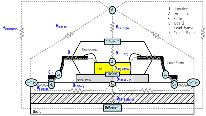
Figure 6. An Example of Thermal Resistance Network
It is vital to spend some time on PCB layout arrangement. Generally speaking, the wider and thicker the PCB trace is, the smaller the thermal resistance. However, if the IC package size is small, the PCB trace width is also restricted. There will be a trade-off between heat transfer and layout rules. For example, the PCB trace of switching node should always be large enough to sustain the current but also be small enough to reduce noise coupling. Adding the thermal Vias in the PCB with multi-layers design is a solution to improve the heat transfer. In the Flotherm simulation tool, it is recommended to transfer the circle Vias to the rectangle Vias to reduce the convergence period. It is simple to use the equation (1) and (2) to complete the conversion. Figure 7 demonstrates the diagram of the conversion.
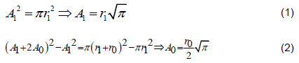
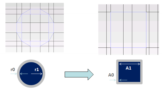
Figure 7. The Conversion of Circle Via to Rectangle Via
4.
Verification
of Thermal Model for Power Management System
After building the thermal models of each component, it is time to do the bench test to verify the accuracy of the thermal models. The verification is into two steps. The first step is to check the accuracy of each component with only one heat source at a time. The second step is to check the accuracy of overall power management system with thermal models.
In Figure 8, the IC thermal model of RT6228 is given. The RT6228 is a HV single Buck converter, and the package type is UQFN-12HL 3x3-56B (FC). The design of flip-chip can reduce the wire bonding impedance to improve the efficiency, and will also reduce the thermal resistance from die to IC pins. It should be noted that the heat generation region of the IC thermal model will be located at the area of internal power MOSFETs. In this case, the heat generation region is located at the bottom half of die. If there are multiple rails in one chip, like PMIC, there will be multiple heat sources. In that case, the heat region should be separated according to the location of each rail.
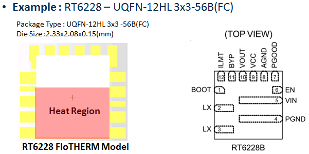
Figure 8. The IC Thermal Model of RT6228
The thermal model of RT6228 EVB is shown in Figure 9. The layout of thermal model is done according to the actual EVB (left of Figure 9). It is a 1oz four-layer design, and the EVB size is 100mm x 72mm. Many thermal Vias are placed in the IC GND and VIN planes to improve the heat transfer to other layers. Because of power and ground planes are major factors to affect the heat transfer, the other control loop traces can be simplified in the PCB thermal model.
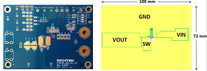
Figure 9. The Thermal Model of PCB
Since the IC cannot work without outer components, the generation of heat source on the chip is a problem. The alternative method is to inject a constant current through the body diode of internal power MOSFET. In order to confirm the accuracy of thermal model at different power dissipation, there are three different levels of injecting current to heat the die. Table 3 shows the verification results of IC thermal model, and the case temperature comparison between simulation and experiment. In this experiment, the current is injected into the body diode of the high-side MOSFET to generate power dissipation, and the ambient temperature is about 25°C. The results show that there is only 2% temperature deviation between the simulation and the experiment.
Table 3. Verification of IC Thermal Model
|
Product
|
VSW-VIN (V)
|
ISW-VIN (A)
|
PD_IC
|
TA (°C)
|
TC_measured (°C)
|
TC_simulated (°C)
|
|
IC Power Loss (W)
|
|
RT6228
|
0.706
|
1.998
|
1.411
|
25.8
|
81.6
|
81.9
|
|
0.688
|
2.998
|
2.063
|
26.3
|
109.2
|
107
|
|
0.671
|
3.997
|
2.682
|
26.4
|
136
|
133
|
The inductor thermal measurement is shown below. Similar to the verification of IC thermal model, the inductor is placed on the PCB, and the heat generation source is the inductor copper wire. The power dissipation is generated by the DCR of inductor winding by injecting the current through the wire. The power loss of inductor can be calculated by multiplying the differential voltage on the two sides of inductor with the injected current. Finally, the verification results are shown in Table 4, and the temperature deviation between measurement and simulation is around 3%.
Table 4. Verification of Inductor Thermal Model
|
Part
|
PD_L (W)
|
TA (°C)
|
TC_meas (°C)
|
TC_sim (°C)
|
|
MMD-10DZ-1R0M-X1
|
1.439
|
26.2
|
68.4
|
69.7
|
|
0.398
|
26
|
39.8
|
38.6
|
Furthermore, here are some tips need to take care of when measuring the case temperature on inductor by thermal imager (Fluke Ti450). Because the reflection coefficient of inductor package is higher than IC package, the IR measurement will be inaccurate. In order to reduce the reflection coefficient of inductor, sticking a piece of black electrical adhesive tape on inductor surface will help to increase emissivity. Figure 10 is an example of inductor temperature measurement. The EVB is placed in a sealed box for still air condition, and the thermal coupler is used for monitoring the ambient temperature in the box. When using the thermal imager for measurement, properly adjust the focus length is essential for accuracy. In addition, wait for thermal balance at least 15 minutes in each test condition.
Figure 10. Experiment Setup for Inductor Temperature Measurement
In previous steps, the thermal model accuracy of each component was verified. In the next step, all of these components will be combined to confirm the complete power management system. The RT6228 can support output voltages from 0.6V to 5V by adjusting the output feedback resistor. To verify the thermal model with different power dissipation, there are two experimental cases to verify the thermal model. The detailed simulation and experiment parameters are listed in Table 5 andTable 6. In each test condition, the power dissipation has been divided into three components: the power loss of IC, the power loss of inductor and the power loss of PCB trace. Therefore, the simulation setup will depend on the distribution of power dissipation. Furthermore, all cases are done at the ambient temperature of 25°C. Simulation and experiment results are shown in Figure 11 and Figure 12. For case 1, the output voltage is 3.3V and load condition is 6A. The power loss of IC, PD_IC, is 1.73W and the power loss of inductor, PD_L, is 0.93W and the power loss of PCB, PD_PCB, is 0.3W. The power loss of inductor includes copper loss and core loss, where the copper loss is calculated through IL2xDCR and core loss can be found on inductor manufacture’s datasheet. In this case, the inductor DCR is 3.3mW and core loss is around 0.81W. The power loss of PCB is calculated through IPCB2xRPCB, where the PCB trace resistance can be divided into two parts: one is the trace resistance from input capacitor to VIN pin, which is around 4mW, and another one is the trace resistance from the SW pin to output capacitor, which is around 8mW. Then the IC power loss is calculated from (PD_IC = PD_TOTAL – PD_L – PD_PCB). Comparing the simulation result with actual measurement experiment result, the case temperature of IC is almost the same and the inductor temperature has small deviation less than 5%. For case 2, the output voltage is 1V and load condition is 6A. The power loss of IC, PD_IC, is 1.53W and the power loss of inductor, PD_L, is 0.286W and the power loss of PCB, PD_PCB, is 0.3W. In this case, the inductor DCR is 3.3mW and core loss is around 0.167W. The PCB trace resistance remains the same as in case1. Comparing the simulation result with experiment result, the case temperature of IC has only 2% deviation, and the inductor temperature has small deviation less than 5%.
Table 5. Simulation and Experiment Parameters of Case 1
|
Thermal Model
|
Test Condition
|
|
Chip
|
RT6228
|
VIN (V)
|
19
|
VOUT (V)
|
3.3
|
IOUT (A)
|
6
|
|
Inductor
|
MMD-10DZ-1R0M-X1-RI
|
Power Dissipation
|
|
PCB
|
RT6228_UQ3_12L_V2
|
PD_IC (W)
|
1.73
|
PD_L (W)
|
0.93
|
PD_PCB (W)
|
0.3
|
Figure 11. Simulation and Experiment Results of Case 1
Table 6. Simulation and Experiment Parameters of Case 2
|
Thermal Model
|
Test Condition
|
|
Chip
|
RT6228
|
VIN (V)
|
19
|
VOUT (V)
|
1
|
IOUT (A)
|
6
|
|
Inductor
|
MMD-10DZ-1R0M-X1-RI
|
Power Dissipation
|
|
PCB
|
RT6228_UQ3_12L_V2
|
PD_IC (W)
|
1.53
|
PD_L (W)
|
0.286
|
PD_PCB (W)
|
0.3
|
Figure 12. Simulation and Experiment Results of Case 2
5.
Summary
In this application note, the modelling and verification of thermal model for power management system has been explained. The development of IC, inductor and PCB thermal models has been described in the report. The verification results show small deviations between simulation and measurement. Finally, with the accurate thermal model simulation, the thermal behaviour of the application can be predicted, and thermal problems like overheating can be prevented. This will be beneficial to shorten development time and avoid extra cost due to trial and error.